New Method for Inexpensive Mass Manufacturing of Micro-LED Displays
Micro-LED displays have many applications, as it is a preferred flat-panel display technology for mobile phones, wearable smart watches, micro-projectors, ultra-high-definition televisions, and virtual/augmented reality. The first inventors of the technology were the research group of Hongxing Jiang and Jungyu Lin of Texas Tech University while there were still at Kansas State University. That was way back in 2000. Micro-LED displays provide better contrast, energy efficiency, and response times than LCD technology. Moreover, the technology is capable of high-speed modulation.
Micro-LED displays consist of arrangements of microscopic LEDs creating separate pixel elements. Compared to common LCD displays, they greatly reduce energy consumption, a high contrast ratio, and pixel-level light control. Another advantage of micro-LEDS is a longer lifetime over OLEDs (organic light-emitting diodes) because of their inorganic nature. This property allows micro-LEDS to display brighter images while reducing the danger of screen burn-in.
High production cost
While micro-LED displays are a better product, the high cost of production prevents them from being mass-produced. This is due to the complicated manufacturing process, the multiple participants of the supply chain, the non-standardized equipment and process, and the unstable and immature yield output and management. The technology’s most significant challenge is the assembly. Putting the thousands of components together drives up the cost of micro-LED production. Despite this setback, the 2025 industry revenue projection is about $7 billion.
Several electronics manufacturers sell micro-LED video walls, while others are presenting prototypes. Still, the challenge is for the technology to enter into mass production to reduce manufacturing cost mass transfer.
Possibility of mass production
A research team from the University of Strathclyde in the UK has developed a continuous roller printing method that could precisely transfer thousands of microscopic semiconductor devices in a single run. The process could lead to the creation of large-scale arrays of optical parts. Thus, the method could likewise be used to produce micro-LED displays quickly.
In their demonstration, the research team showed a continuous roller printing process capable of picking up and transferring more than 75,000 micrometer-scale semiconductor devices in a single roll. The process was highly accurate.
As the electronics, communication, and entertainment market continuously demand better quality products at lower costs, this research is timely. There is high demand for micro-LED displays because they can provide highly accurate color rendering with high speed and resolution while consuming minimal power. The displays apply to various formats, from large displays and augmented and virtual reality devices to smartphone screens.
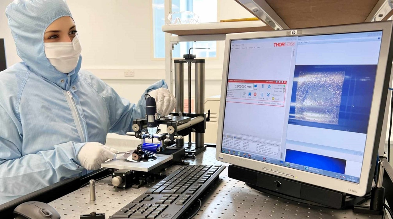
According to the head of the research team, Eleni Margariti, international teams, including industry and academic research groups, are tackling the challenge of transferring micro-meter scale semiconductor devices into a wide range of receiving platforms. The roller-based printing process the UK team developed offers a way to attain it in a scalable way and meet the required accuracy demanded by the application.
She added that the new roller printing technology could meet the designed device layout with a less-than-one-micron accuracy. The setup is simple and inexpensive, allowing the printer to be constructed in locations where resources are limited.
Further applications
The new printing process has various applications and can be used for other device types such as silicon, printed electronics like antennas, sensors, and transistors for wearable and flexible electronics, radio-frequency identification tags, and smart packaging. The process can also be used for photovoltaic production and biomedical applications such as tissue engineering, biosensors, and drug delivery systems.
Large-scale yet simpler process
The complexity of manufacturing semiconductor devices prevents the mass production of the technology, where compatibility between materials is a key issue. Ms. Margariti explained that her team wanted to improve the transfer of large numbers of semiconductor devices from one substrate to another.
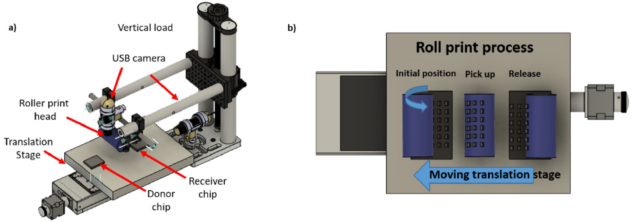
Their approach begins with a suspended array of micro devices loosely attached to their growth substrate. A cylinder with a slightly sticky silicone polymer film rolls over the suspended array, and the sticky polymer film detaches the devices from the substrate and transfers them to the drum.
They achieve high printing accuracy by carefully selecting the properties of the silicone and receiving substrate surface. They also control the speed and mechanics of the rolling process. Thus, they can preserve the spatial arrangement from the original substrate. The system includes a custom analysis method.
Next step
The research team is fine-tuning the system to improve its printing accuracy further and increase the number of devices it can transfer in one go. They also want to test the system’s capability to transfer different types of devices onto similar receiving platforms and other possibilities.