Japanese Scientists Use Novel Laser Technique to Slice Semiconductors from Diamonds
In the semiconductor industry, silicon is still the prime material. However, this may soon change, as Japanese scientists created a method to slice diamonds into wafer-thin pieces using a new laser technique.
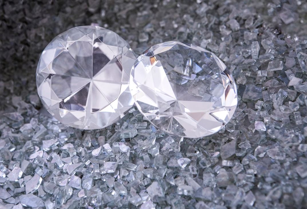
While silicon is a primary semiconductor material, diamonds are fast becoming one of the most promising materials because the carbon in diamond form has a wider band gap. Diamonds have several tech applications, including power conversion and fast telecommunications. But the mineral is difficult to work with because of its hardness. Thus, they are prone to cracking when cutting wafer-thin slices from them.
New laser cutting technique
However, Chiba University of Japan scientists claim they have developed a new way to create diamond wafers using lasers. They recently announced they have created a radical laser-based method to slice diamonds easily.
Materials with wide band gaps, like diamonds, allow semiconductors to perform more efficiently at higher temperatures and voltage frequencies, which is impossible using only silicon. With the wider band gap of diamonds, it is possible to build ultra-efficient power circuitry, which could benefit the train and electric vehicle industries.
But since diamond is famous for its hardness and tendency to crack, they were considered unsuitable for producing semiconductor wafers, which Japanese scientists want to overcome.
In the past, researchers have had to synthesize diamond wafers, which is a very expensive process. But the experiments of the Chiba University School of Engineering research team headed by Prof. Hirofumi Hidai show that lasers can cut wafer-thin diamond slices by influencing the way the mineral cracks along a specific crystallographic plane.
Prof. Hidai explained that their technique produces high-quality diamond wafers at low cost. He said that their process involves using laser light to modify specific regions of the diamond into amorphous carbon. The latter has a lower density than the diamond. Thus, the tendency to crack is minimized.
Another process the Japanese scientists worked on was controlling the formation of cracks through the diamond. They need to form along the intended plane to create a feasible wafer. With the help of lasers, they created a grid-like pattern of the crack-prone areas of the diamond, which provided them a guide in the crack propagation along the identified path. They use a tungsten needle set against the diamond’s side while slicing the wafer. The tungsten needle remains in place until the wafer breaks from the main piece.

Interest from other groups
The University of Chiba and Professor Hidai are not the only ones aiming to harness the dense lattice of a diamond’s carbon atoms to power next-gen communications and computing technologies.
A few months back, Amazon Web Services (AWS) and Element Six, a De Beers subsidiary, teamed up to develop synthetic diamonds. They intend to use these in quantum key distribution by engineering defects into the diamond. They call these defects color centers, which can absorb photons that contain quantum information, which the material can emit later. Amazon thinks the process can harness the phenomenon to develop repeaters that can extend the reach of quantum key distribution to the company’s network worldwide. According to the head of AWS, Antia Lamas-Linares, quantum networks will be available in a few years.
Prof. Hidai said their new proposed method could be a crucial step towards turning diamonds into a desirable semiconductor material for more efficient technologies in the future. The professor also explained that their method of slicing diamonds would produce high-quality wafers cheaply.